Research
Electrochemical Nanoimprinting
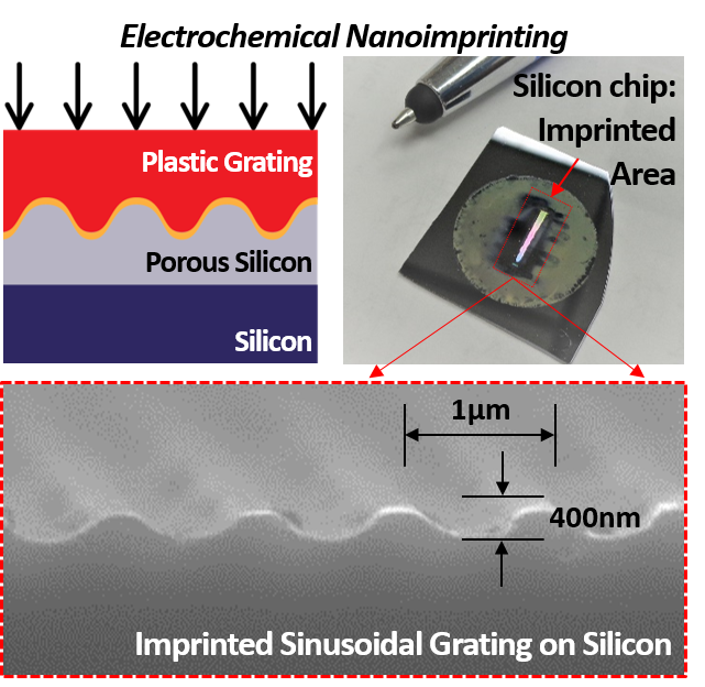
Intro. Electrochemical nanoimprinting is a top-down method for patterning 3D nanoscale features with sub-20 nm nanometer resolution onto inorganic semiconductors such as silicon and porous. It is capable of inch-scale parallel patterning that avoids need for lithographic patterning for each substrate to be patterned by using a reusable imprinting stamp and wet chemistry. At the core of this patterning technique lies the use of a noble metal-coated stamp immersed in an acid and oxidizer mixture and brought in contact with a Si substrate to selectively induce etching of the silicon at the contact interfaces (as shown on your right). Unlike previous configurations of nanoimprinting, it requires minimal mechanical forces and no resulting plastic deformation or residual stresses of either the substrate or stamp materials. As a result, patterns from a single polymeric mold can be replicated innumerous times onto silicon wafers much like mold replication takes place in soft-lithography. Read more.
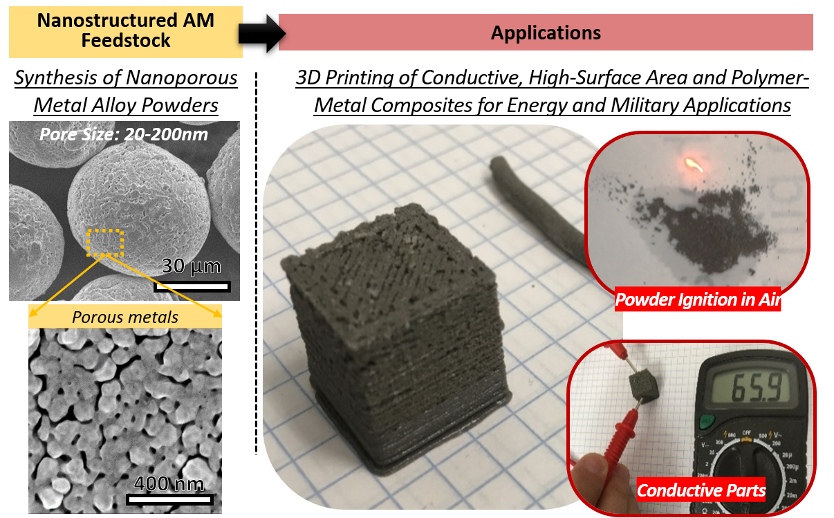
Intro. Multi-material printing has been a highly desirable capability in the additive manufacturing community because it can enable heterogeneous materials to be integrated into complex architectures with added multi-functionallity. The world is full of heterogeneous materials joined in a variety of ways to combine the properties of polymers, metals and ceramics into functional products everyday. So, why don’t we see 3D printing strategies that can 3D print polymers, ceramics and metals concomitantly (hint: “manufacturing challenges”)?
Our group is particularly interested in nanoporous metals for it has high-surface area and catalytic performance relevant to 3D print (i) energetic materials for military applications, and (ii) energy storage & harvesting devices (e.g. fast-discharging batteries and nanostructured photoanodes for hydrogen production). Read more.