Research: Electrochemical Nanoimprinting
1) Manufacturing Geometrically Complex Hierarchical Micro- & Nanostructures in Silicon for High-Performance IR Optics
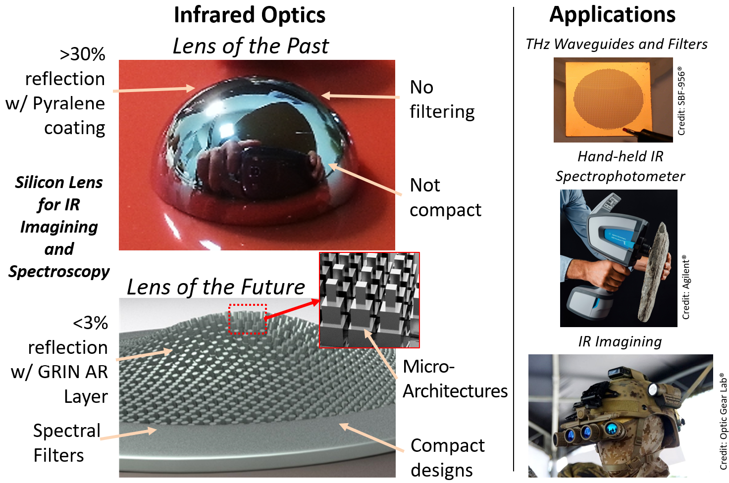
Application. Freeform 3D single-crystal silicon micro- and nanostructures offer the opportunity to topologically control light using ray optics and sub-wavelength engineering of light-matter interaction. In turn, they enable realization of a myriad of optical devices such as classical elements (e.g. homogenizers, diffraction gratings and microlens arrays), metasurface-based elements for silicon photonics, x-ray flat-lenses, optical resonators for biosensing, biomimetic lenses & imagers, and graded-index materials as anti-reflective and high-emissivity surfaces for photovoltaics and space applications, respectively.
Manufacturing Challenges. However, existing parallel bulk micromachining processes for silicon do not offer the ability to fabricate freeform structures with specific challenges when it comes to hierarchical micro and nanoscale 3D features. At the root of this challenge lies the indirect nature of existing parallel micromachining strategies that combine sacrificial templates – manufactured on a wafer-scale by gray-scale lithography with top-down processes such as deep reactive-ion etching to etch 3D micro- and nanostructures. While this process combination led to sub-10 nm line resolution in planar memory devices, it cannot replicate such resolution out-of-plane due to (a) poor control over mask selectivity during etching, (b) roughness produced via scalloping effects, and (c) etch rate dependence on feature size in dry etching (Figure 1).
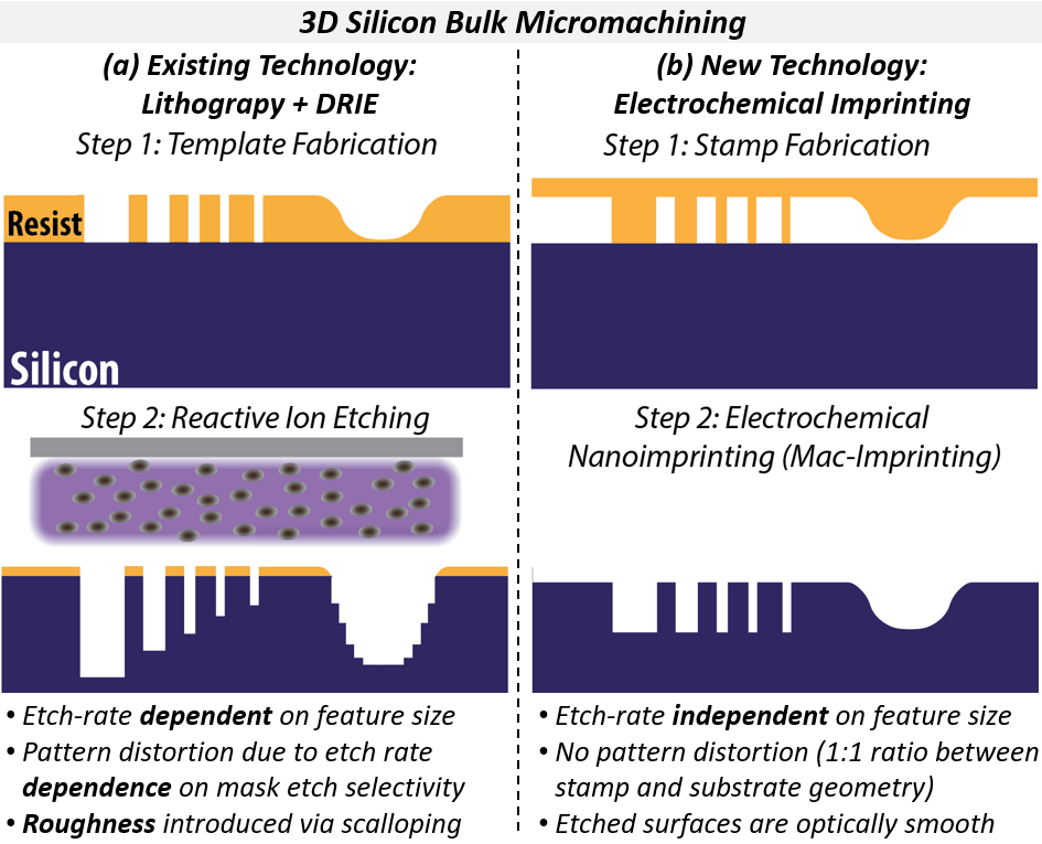
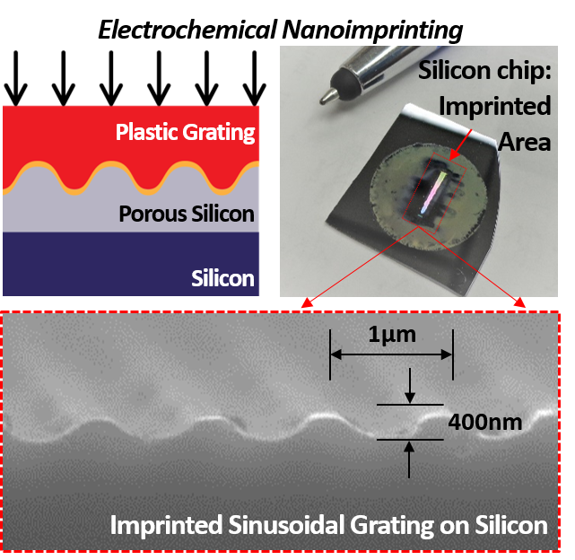
Innovation. Electrochemical nanoimprinting is a top-down method for patterning 3D nanoscale features with sub-20 nm nanometer resolution onto inorganic semiconductors such as silicon and porous. It is capable of inch-scale parallel patterning that avoids need for lithographic patterning for each substrate to be patterned by using a reusable imprinting stamp and wet chemistry. At the core of this patterning technique lies the use of a noble metal-coated stamp immersed in an acid and oxidizer mixture and brought in contact with a Si substrate to selectively induce etching of the silicon at the contact interfaces (as shown on your right). Unlike previous configurations of nanoimprinting, it requires minimal mechanical forces and no resulting plastic deformation or residual stresses of either the substrate or stamp materials. As a result, patterns from a single polymeric mold can be replicated innumerous times onto silicon wafers much like mold replication takes place in soft-lithography.
Key Related Publications:
- Sharstniou, A., Niauzorau, S., Hardison, A., Puckett, M., Ryckman, J., Krueger, N., Azeredo, B.*, “Roughness suppression in electrochemical nanoimprinting of Si for applications in silicon photonics”, Advanced Materials, accepted, 2022
- Niauzorau, S., Kublik, N., Sharstniou, A., Sampath, V., Bandarenka, H., Azeredo, B., “Electroless Dealloying Of Thin-Film Nanocrystalline Au-Ag Alloys: Mechanisms Of Ligament Nucleation And Sources Of Its Synthesis Variability”, ACS Applied Materials & Interfaces, 14, 15, 17927-17939, 2022
- Sharstiniou, A., Niauzorau, S., Ferreira, P., Azeredo, B., “Electrochemical Nanoimprinting of Silicon”, PNAS, 2019
- Sharstniou, A., Niauzorau, S., Azeredo, B., “Direct Nanoimprinting Of Silicon: A Direct Patterning Approach”, Novel Patterning Technologies, SPIE Advanced Lithography, San Jose, California, 2018
- Azeredo, B., Lin, Y., Avagyan, A., Hsu, K., Ferreira, P., “Direct Imprinting of Porous Silicon via Metal-Assisted Chemical Etching”, Advanced Functional Materials, Vol. 26, 2016
- Azeredo, B., Hsu, K., Ferreira, P., “Direct Electrochemical Imprinting of Sinusoidal Linear Gratings into Silicon”, Proceedings of the 2016 Manufacturing Science and Engineering Conference (ASME-MSEC), Vol. 1, Blacksburg, VA, 2016